In a recently-published review paper titled Conductive Oxide Interfaces for Field Effect Devices we briefly describe oxide 2D electron gases (2DEGs), and then take a journey from the first devices published in 2012 all the way to the most recent and exciting advancements. In merely 7 years, these transistors have reached the short-channel effect (SCE) limits (60 nm channels), 700k transistors were manufactured on a single chip, functional circuits and NOT gates demonstrated, and the onset of 3D devices explored. A few months ago, a series of revolutionary papers from Korea demonstrated oxide 2DEGs that are all prepared by atomic layer deposition, opening scalable routes for exciting new applications and 3D integration on top of silicon technology (“building penthouses on top of chips”).
(Email for a free copy)
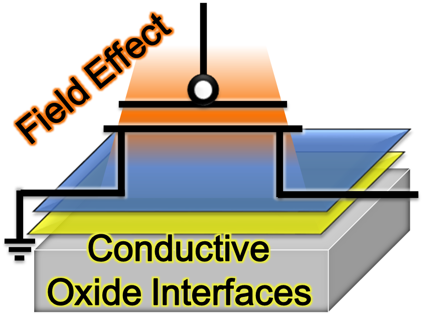
Conductive oxide interfaces for field effect devices (cover image for Advanced Materials Interfaces)
Quoting from the abstract:
“By presenting an overview of the state of the art, it is hoped to inspire new applications for these diverse new capabilities. The journey of conductive oxide interfaces from fundamentals to technology may be viewed as a prototype for the future maturation of other systems of emergent physics and novel materials from labs to devices.”